

Hall Current Sensor Factory: Inside Precision Manufacturing and Quality Control
2026-08-29
Most people never see the tiny components that keep our power grids stable, but inside every modern electrical system, Hall current sensors are quietly doing the heavy lifting. At Xiasen, precision manufacturing isn't just a buzzword—it's a daily obsession. From micron-level core winding to relentless thermal cycling tests, every sensor that leaves the factory carries a promise of accuracy and durability. Step inside with us to see how rigorous quality control turns raw materials into the unsung guardians of your devices.
Where Sensor Cores Take Shape: A Walk Through the Production Floor
Walking onto the floor, the first thing that hits you is the low, steady hum of air handlers pushing filtered air through ceiling vents. Workers in pale blue bunny suits and face masks move between stations, each one logged by a barcode scanner before touching anything. The cores begin as thin ceramic wafers, lifted from cassettes by vacuum wands and carried to inspection stages. No bare hands ever make contact with the surface.
At the lithography bays, patterns are projected onto photoresist under orange light, because ordinary white light would expose the coating too early. A technician leans into a microscope, adjusts the stage by micrometer clicks, then signs off on the batch. Next door, deposition chambers glow faintly as layers of platinum and silicon nitride build up one atom at a time. The air carries a faint solvent smell, though the scrubbers leave it almost neutral.
By the end of the line, each core sits in a test socket, wired to a bank of analyzers. Live output curves scroll on a screen while a probe needle touches the contact pads. Rejects are rare, but any that fail are pulled aside and marked with a small red dot. Finished cores go into black antistatic trays, each one sealed with a desiccant pack before moving to the cold vault. The walk takes twenty minutes, but the cores have spent six hours in this room.
Calibration Rooms and the Pursuit of Microvolt Accuracy
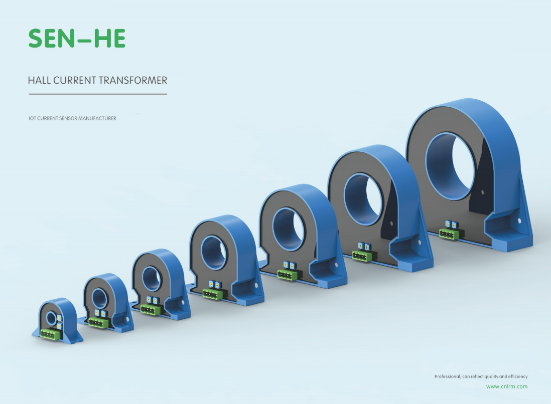
Inside a calibration room, every cable is routed with deliberate curvature to avoid parasitic capacitance shifts that could nudge a reading by a few microvolts. The temperature sits at 23.0 °C, but the real battle is against thermal EMFs at every connector junction where dissimilar metals meet. Technicians use low-thermal solder and keep their hands off the binding posts, because even body heat can create a gradient that masquerades as signal. It is less about making things perfect and more about knowing exactly how imperfect each link is.
Chasing microvolt accuracy means accepting that the floor above is walking a different rhythm—vibration from a distant HVAC unit can modulate a sensitive null detector. Instead of chasing ghosts, metrologists map those disturbances: they log the spectral signature of line noise, plot drift over hours, and build a noise budget that quantifies every contributor from resistor self-heating to connector oxidation. The calibration room becomes a living document of uncertainty, not a sterile box.
What separates a good room from a great one is rarely the equipment list; it is the refusal to trust a single reading. Interchanging leads, reversing polarity, soaking standards for days, and comparing against two independent references are the quiet rituals that expose microvolt-level lies. In that environment, a 10 µV discrepancy is not an error to erase but a clue—a fingerprint of a thermocouple effect, a leaky guard, or a ground loop hiding in plain sight.
Material Choices That Define Long-Term Drift Performance
When engineers talk about drift, they are rarely describing a sudden failure. It is the slow, almost invisible migration of a signal or mechanical position over weeks, months, or years of continuous operation. The materials chosen at the design stage quietly decide whether that drift stays within a few parts per million or accumulates into a costly calibration cycle. Metals with high thermal expansion coefficients, for instance, will expand and contract with every ambient temperature swing, slowly working against even the most precise electronic adjustments. Yet the issue is not simply about picking the most stable material on paper; it is about understanding how two adjacent materials push and pull against each other when bonded, clamped, or soldered.
Consider the humble resistor network in a precision analog front end. A designer might specify thin-film nichrome for its low temperature coefficient, only to discover that the alumina substrate beneath it introduces a hysteresis loop with every thermal cycle. The drift does not come from the resistive element itself, but from the mechanical stress transferred through the interface. Choosing a matched pair of materials—say, a silicon-chromium film on a glass-ceramic substrate with nearly identical expansion behavior—can reduce that stress-induced drift by an order of magnitude. This kind of pairing is not found in a datasheet; it emerges from testing candidate stacks under repeated thermal shock and long-term bias.
Long-term drift is also shaped by materials that seem inert but are not. Epoxy encapsulants outgas volatile compounds for years after cure, subtly changing the dielectric constant around high-impedance nodes. Solder joints develop intermetallic growth layers that alter contact resistance, especially when tin meets gold. The practitioners who get drift under control are not the ones who chase the lowest specified coefficient, but those who treat every material interface as a dynamic system. They ask what happens after ten thousand power cycles or one thousand hours at 85°C and 85% relative humidity. The answer is rarely found in a single material property; it lives in the interaction between the chosen metal, ceramic, polymer, and the exact sequence of assembly steps.
Automated Optical Inspection: Catching Flaws Before They Leave
Every board that passes through the line carries a silent risk: a hairline solder crack, a tombstoned capacitor, or a misaligned connector invisible to the naked eye. Automated Optical Inspection steps in at the exact moment these defects would otherwise slip downstream. Using high-resolution cameras and layered lighting, the system scans each assembly in seconds, comparing every pad, fillet, and component edge against a golden reference model. The result is not just detection, but a precise report of where the flaw lives—so rework happens now, not after the product ships.
What makes modern AOI stand out is its ability to learn the line's own fingerprint. Early runs teach the machine which variations are harmless and which are trouble. False calls drop, real catches rise. And because inspection happens inline, the data feeds back instantly: a trending bridge on pin five of a specific connector prompts a stencil tweak before the next panel loads. That loop between seeing and correcting is where yield quietly improves.
In practice, the best AOI setups don't just find flaws—they shorten the distance between flaw and fix. Operators see heatmapped images, not cryptic coordinates. A tech can reach for the right tool before the board cools. And when the line runs fast, that speed of feedback is the difference between catching one bad board and catching a whole shift of them.
Environmental Stress Screening: How Sensors Earn Their Ratings
A sensor's printed temperature range or vibration tolerance isn't a guess. It comes out of environmental stress screening (ESS), a punishing series of tests that push prototypes and production units far beyond typical operating conditions. The goal isn't to simulate normal use—it's to expose weaknesses that would otherwise show up months later in the field.
Thermal cycling chambers alternate between extreme cold and heat, sometimes swinging 100°C in minutes, to crack solder joints and delaminate substrates. Shaker tables hammer sensors with random vibration profiles while humidity chambers and salt spray test corrosion resistance. Each failure during screening triggers a root-cause analysis and a design or process tweak, then the cycle repeats. Over time, the mean time between failures shifts upward because marginal components never make it past the factory floor.
The rating stamped on the datasheet is the result of this iterative torture. A sensor rated for -40°C to +125°C has survived repeated excursions to those limits, not just a single pass. Buyers who treat those numbers as earned, rather than claimed, understand why screened sensors cost a bit more—and why they rarely surprise you in the middle of a winter startup or an engine bay heat soak.
Traceability from Wafer to Final Test Report
In semiconductor manufacturing, traceability from wafer to final test report hinges on a unique identifier assigned to every wafer at the start of fabrication. This identifier, often laser-scribed as a wafer ID, stays with the wafer through thinning, dicing, and die bonding. As individual die are singulated and placed onto substrates, the system records which wafer each die came from, linking the wafer ID to package-level serial numbers.
Once packaged units move into final test, automated handlers read the package markings and associate each unit with its complete manufacturing history. Test data—including pass/fail bins, parametric measurements, and any retest results—is logged against the same serial number. This creates a continuous data chain: a specific failing unit can be traced back to its original wafer lot, fab equipment, and even process step, enabling root cause analysis without losing context.
The final test report aggregates these records into a per-unit or per-lot summary. It includes the wafer map, assembly disposition, electrical test outcomes, and any deviations. Auditors and quality engineers rely on this report to verify that every shipped part meets specifications and that no untracked material entered the flow. In high-reliability sectors like automotive or medical, this level of traceability is not optional—it is required for compliance and customer confidence.
FAQ
A dedicated hall current sensor factory tunes every stage around the magnetic core's behavior. Instead of simply assembling parts, the line controls air gap geometry during core placement, uses closed-loop flux calibration per unit, and matches the Hall element's temperature coefficient to a compensation network before potting. That level of process integration is hard to replicate in a general-purpose electronics line.
Each sensor runs through an automated flux loop calibration where the output is compared against a reference current shunt traceable to national standards. The line adjusts the internal gain resistor or trims the ASIC registers on the fly, so sensitivity variation stays within a tight band of ±0.3% across thousands of units.
Before shipping, every sensor must pass high-potential isolation testing at 3kV, a temperature cycle from -40°C to 125°C, zero-offset monitoring after warm-up, and a vibration sweep. Then a random sample is pulled for destructive teardown to verify potting void ratio and solder joint integrity under X-ray.
The Hall element's intrinsic sensitivity drifts with temperature, so without correction, a 100A reading could shift by several amps between cold start and full load. The factory pairs a negative-temperature-coefficient thermistor with a digital compensation curve stored in EEPROM, keeping the total drift under 50 ppm per degree Celsius.
The AOI stations check for solder bridging on the ASIC pins, verify that the magnetic core hasn't shifted during reflow, and confirm that the leadframe coplanarity is within 0.1mm. This prevents uneven air gaps that would introduce non-linearity or false triggering in the final current measurement.
After the core is annealed and mounted, a short high-current pulse demagnetizes any residual field. Then a programmable ASIC applies a zero-offset correction while the sensor sits in a magnetically shielded chamber. That two-step process removes most of the hysteresis error before the sensor is even potted.
Yes. The factory offers custom winding turns, alternate core materials for high-frequency operation, and selectable output interfaces such as ratiometric analog, 4-20mA current loop, or SENT digital. Small pilot lots can be run in under two weeks, with the same calibration and burn-in protocols as volume production.
Sensors undergo 85°C at 85% relative humidity for 1,000 hours, rapid thermal shock between -40°C and 125°C for 500 cycles, and a high-temperature operating life test at 125°C with full rated current. Only after these tests show less than 0.5% sensitivity shift and no insulation breakdown does the design get released for mass production.
Conclusion
On the production floor, the first thing you notice is the quiet order of it. Sensor cores don't start as sensors at all, but as strips of grain-oriented silicon steel or permalloy, cut and stacked under presses that hold tolerances to the micron. Each batch moves with a paper traveler, not just for scheduling but because the Hall element's offset voltage will later be matched to the core's exact air gap. In the calibration rooms, shielded from ambient fields, every sensor sits in a thermal chamber for hours while a programmable current source steps from milliamps to hundreds of amps. The goal isn't a single reading but a drift curve flat to within a few microvolts across temperature. If a unit drifts, the technician doesn't tweak a trim pot; they trace the batch back to the wafer lot and the core annealing run.
Material choice is where long-term performance is decided. Cores with high nickel content cost more but hold linearity over a decade; cheaper alloys show measurable offset drift within two years. After assembly, every sensor passes under automated optical inspection cameras that look for solder voids, hairline cracks in the epoxy, or a misplaced Hall die. Then comes environmental stress screening: thermal cycling from -40°C to +125°C, vibration sweeps, and humidity soak at 85°C/85% RH. Units are powered throughout, and any glitch in output is logged with the exact cycle number. Finally, traceability closes the loop. Each final test report carries not just the measured accuracy but the serial numbers of the wafer, the core batch, the assembly operator, and even the calibration fixture used. That's how a sensor earns its datasheet rating, not by statistical sampling but by surviving the same gauntlet every time.
Contact Us
Contact Person: Liu Mengyang
Email: [email protected]
Tel/WhatsApp: 8618727589233
Website: https://www.cnlrm.com/en/